Introduction
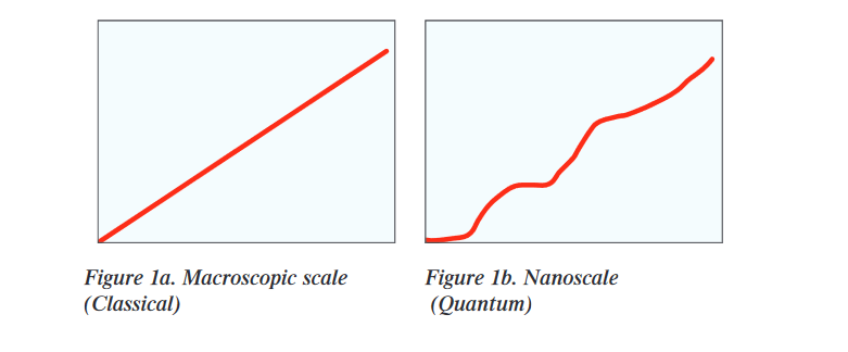
As modern electronics continue to shrink, researchers are increasingly looking to nano technology as the basis for the next breakthrough in device size and power consumption. Indeed, as semiconductor structures are made smaller and smaller, the distinction between small silicon geometries and large molecules becomes blurred. Approached from either direction, the consequences are the same. Quantum behavior such as tunneling begins to play an important role in the electrical characteristics. In the macroscopic world, conductors may have obeyed Ohm's Law (Figure 1a), but in the nanoscale, Ohm's definition of resistance is no longer relevant (Figure 1b). Because the slope of the I-V curve is no longer a fundamental constant of the material, a detailed measurement of the slope of that I-V curve at every point is needed to study nanodevices.This plot of differential conductance (dG = dI/dV) is the most important measurement made on small scale devices, but presents a unique set of challenges.
Who Uses Differential Conductance?
Differential conductance measurements are performed in many areas of research, though sometimes under different names. When used to measure the electron energy structure of small devices such as quantum dots, nanoparticles, or artificial atoms, it is sometimes referred to as electron energy spectroscopy. When used to perform non-contact measurements on surfaces within a scanning tunneling microscope, it may be called tunneling spectroscopy.When studying ultra-small semiconductor structures or nanotubes with semiconducting properties, it might be called a density of states measurement. Still other researchers refer to it more mathematically, as the derivative of the I-V curve, or simply dI/dV or ΔG. It can be used to understand conduction phenomenon in cryogenic environments or to observe and predict the conditions when tunneling is more likely to occur. A few examples of the device types that can be studied this way are Schottky diodes, tunnel diodes, and single electron transistors. The fundamental reason differential conductance is interesting is that the conductance reaches a maximum at voltages (or more precisely, at electron energies in eV) at which the electrons are most active. This explains the common use of the name energy spectroscopy. This is also why dI/dV is directly proportional to the density of states and is the most direct way to measure it.
Existing Methods of Performing Differential Conductance
While there is no standardized technique to obtain differential conductance, almost all approaches have followed one of two methods:
(1) Perform a current-voltage sweep (I-V curve) and take the mathematical derivative,
or
(2) Use an AC technique of applying a sinusoidal signal superimposed on a DC bias to the sample. Then use a lock-in amplifier to obtain the AC voltage across and the AC current through the DUT (device under test).
I-V Technique
The I-V sweep technique has the advantage that it is easier to set up and control. It only requires one source and one measurement instrument, which makes it relatively easy to coordinate and control. The fundamental problem is that even a small amount of noise becomes a large noise when the measurements are differentiated.
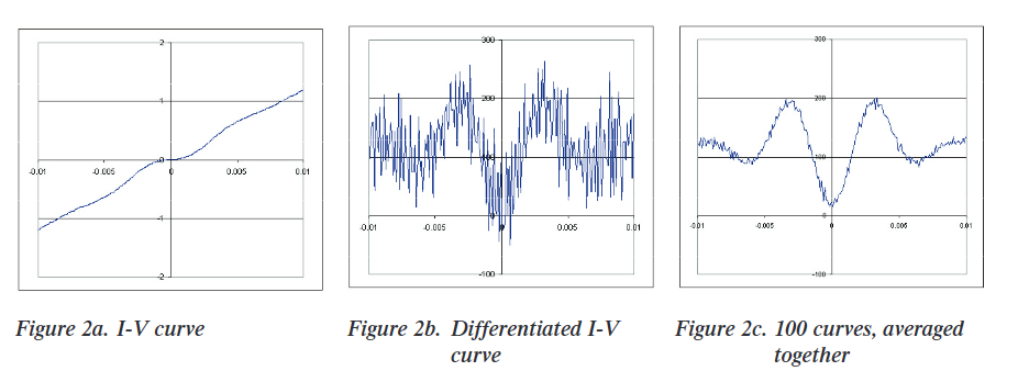
Figure 2a shows an I-V curve, a series of sourced and measured values (V1, I1), (V2, I2), etc. Several techniques can be used to differentiate this data, but the simplest and most common uses the slope between every pair of consecutive data points. For example, the first point in the differential conductance curve would be (I2-I1)/(V2-V1). Because of the small differences, a small amount of noise in either the voltage or current causes a large uncertainty in the conductance. Figure 2b shows the differentiated curve and the noise, which is unacceptably large for most uses. To reduce this noise, the I-V curve and its derivative can be measured repeatedly. Noise will be reduced by , where N is the number of times the curve is measured. After 100 repetitions, which can take more than an hour in a typical application, it is possible to reduce the noise by a factor of 10, as shown in Figure 2c. While this could eventually produce a very clean data set, researchers are forced to accept high noise levels, because measuring 10,000 times to reduce the noise 100x would take far more time than is usually available. Thus, while the I-V curve technique is simple, it forces a trade off between high noise and very long measurement times.
The AC Technique
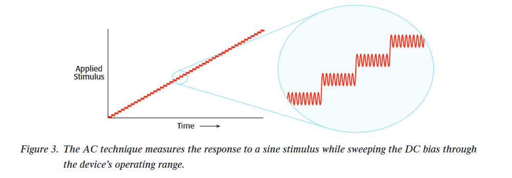
The AC technique superimposes a low amplitude AC sine wave on a stepped DC bias, as shown in Figure 3. The problem with this method is that, while it provides a small improvement in noise over the I-V curve technique, it imposes a large penalty in terms of system complexity.
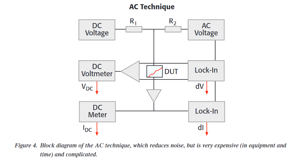
Mixing the AC and DC signals is a significant challenge. It is sometimes done with series resistors and sometimes with blocking capacitors. With either method, the current through the DUT and the voltage across the DUT are no longer calibrated, so both the AC and DC components of the current and voltage must be measured, as shown in Figure 4. A lock-in amplifier may provide the AC stimulus, but frequently the required AC signal is either larger or smaller than a lock-in output can provide, so an external AC source is often required and the lock-in measurements must be synchronized to it.
The choice of frequency for the measurement is another complicating factor. It is desirable to use a frequency that is as high as possible, because a lock-in amplifier's measurement noise decreases at higher frequencies. However, the DUT's response frequency usually limits the usable frequency to 10-100Hz, where the lock-in amplifier's measurement noise is five to ten times higher than its best specification. The DUTs response frequency is determined by the device impedance and the cable capacitance, so long cabling, such as that used to attach to a device in a cryostat, reduces the usable frequency and increases noise, further reducing the intended benefit of the AC technique. Above all, the complexity of the AC method is the biggest drawback, as it requires precise coordination and computer control of six to eight instruments, and it is susceptible to problems of ground loops and common mode current noise.
Another challenge of this method is combining the AC signal and DC bias. There's no one widely recognized product that addresses this issue. Often, many instruments are massed together in order to meet this requirement. Such instrumentation may include a lockin amplifier, AC voltage source or function generator (if not using the reference in the lock-in amplifier), DC bias source, DC ammeter, and coupling capacitor/circuitry to combine AC source and DC bias. In many cases, what researchers are really trying to do is source current, so the series resistors used to combine the AC and DC must be higher impedance than the device, which is unknown until the measurement is made. An example system is shown in Figure 4. Assembling such a system requires, in addition to time, extensive knowledge of electrical circuitry. Time and technical resources often challenge material researchers and students of other disciplines who are interested in characterizing devices.
Conclusions About Old Techniques
In summary, the I-V technique is simple, but noisy. The AC technique has marginally lower noise, but is very complex. Fortunately, however, there is a technique that is both simple and low noise.
Keithley Method for Performing Differential Conductance
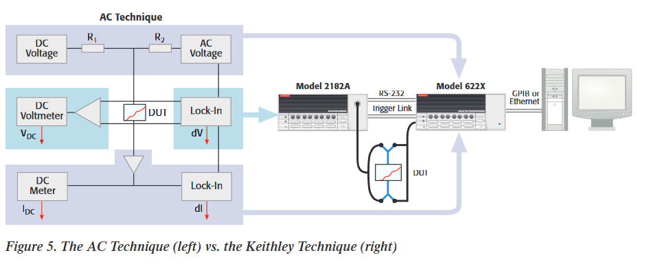
Now there is another approach to differential conductance, a four-wire, source current/measure voltage technique. Keithley is introducing this capability with its Models 6220 and 6221 Current Sources and 2182A Nanovoltmeter. The current sources combine the DC and AC components into one source, with no need to do a secondary measure of the current, because its output is much less dependent on the changing device impedance (Figure 5).
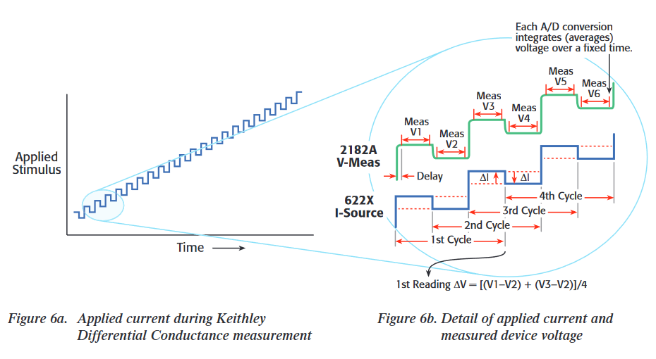
Keithley's method is performed by adding an alternating current to a linear staircase sweep. The amplitude of the alternating portion of the current is the differential current, dI (Figure 6). The differential current is constant throughout the test. The current source is synchronized with the nanovoltmeter via the Trigger Link cable. After measuring the voltage at each current step, the nanovoltmeter calculates the delta voltage between consecutive steps.Each delta voltage is averaged with the previous delta voltage to calculate the differential voltage, dV. The differential conductance, ΔG, can now be derived using dI/dV. The math for this is covered in more detail in the white paper titled "Achieving Accurate and Reliable Resistance Measurements in Low Power and Low Voltage Applications," which is available online at www.keithley.com.
Why Choose the Keithley Method
The new Keithley method for differential conductance provides low noise results at least 10x faster than previous methods. There are many other benefits of selecting the Keithley 6220/6221 Current Source and 2181A Nanovoltmeter to make differential conductance measurements. One is that significantly fewer instruments are required (see Figure 5). The Keithley method requires two instruments (the 6220/6221 and 2182A) while the AC technique requires eight instruments and external circuitry.
Devices must be characterized over a user-defined set of currents (or voltages). When the user defined currents are small, the low current capability of the 622X is unmatched by any user-made system in source accuracy, source noise, and capability to do guarding, which reduces DC leakage and improves system response time. It is also able to source current accurately well below 10pA. Whether or not the current levels are low, the voltage levels are almost always low. The nanovoltmeter's sensitivity, which is superior to lock-in amplifiers, its low 1/f noise, and its ability to compensate for offsets and drift make it a superior solution for differential conductance measurements.
The Keithley method uses four-wire connections, which are desirable because they eliminate voltage errors due to lead resistance or contact resistance. This is of especial concern when the device has regions of low or moderate impedance, because lead resistance may be significant compared to the actual resistance of the device. In a four-wire configuration, there is no current flowing through the sense leads and thus no voltage drop.Essentially, the voltmeter is placed directly across the DUT.
Another key benefit of sourcing current and measuring voltage is that in areas of highest conductance, more data points are collected by sourcing the sweep in equal current steps. Often, these areas are exactly the areas in which researches are most interested. Thus,the data collected with the Keithley method is most detailed around these regions of interest.
As discussed before, the I-V technique can take tens of thousands of measurement sweeps to attain sufficiently low noise. Because of its inherently low sourcing and measuring noise, the Keithley technique requires only one pass, shortening hours of data collection to a few minutes.
In the AC method the speed limitations are a direct result of cable capacitance. Device impedance multiplied by cable capacitance (R × C) is the fundamental system time constant.With three separate instruments connected directly to the device, this capacitance can be extremely high. This means that stimulus cannot be applied to the device at a frequency faster than this time constant. This forces the AC technique to be used at lower frequencies, which results in higher noise due to 1/f effects. With lock-in amplifiers, the lower the frequency used, the greater the measurement noise. The Keithley method, with two instruments connected to the device instead of three as in the AC technique, has an inherently lower cable capacitance. Further, the 6220/6221 provides an active guard, which eliminates the slowing effects of cable capacitance. This greatly improved device settling time results in higher speed and greater accuracy.
Special Cases
Some devices have non-monotonic I-V curves. This behavior is classified into two categories. Both categories are sometimes referred to as NDC (negative differential conductance).
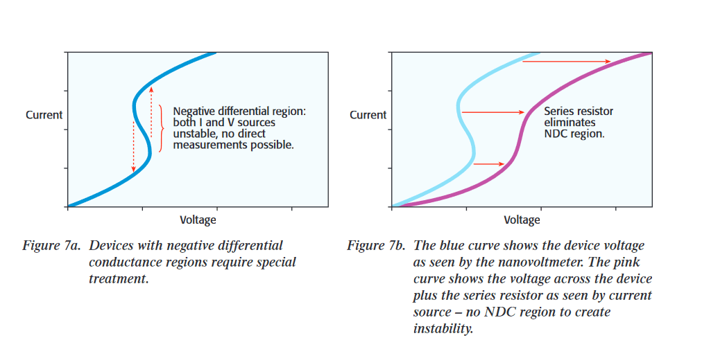
(1) Current Hop - A given voltage may correlate to more than one possible current (Figure 7)
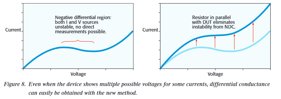
(2) Negative Differential Conductance - A given current may correlate to more than one possible voltage (Figure 8)
Let's look at how the source current/measure voltage differential conductance method can be used with devices that exhibit these types of behaviors.
Current Hop
Some devices exhibit an I-V curve where the current is a multi-valued function of voltage (Figure 7a). The negative differential conductance region cannot be characterized by applying a voltage source, because any regulated voltage source is unstable into negative resistance loads. Instead, a voltage source would produce a hysteresis curve that never traces out the NDC region (dashed lines in Figure 7a). Interestingly, a current source is not stable over this NDC region either, but adding a series resistor in the HI lead presents a composite device to the current source, so that it does not see any NDC region. This resistance must be at least as large as the largest negative resistance throughout the NDC region of the device.
Without any change to the 622x setup, the entire differential conductance curve can be measured because the four-wire configuration connects the nanovoltmeter directly across the device and not the series resistor, whose voltage drop is rejected along with all other lead resistance. This lead resistance, which is normally considered a problem, actually makes full characterization possible with these devices. With Keithley's source current architecture there is no additional measurement required. Other methods require measurements of both device current and voltage in these cases.
Negative Differential Conductance
If the I-V curve exhibits voltage that is a multi-valued function of current, again, neither voltage nor current sources are stable over the NDC region. To stabilize this measurement, it is necessary to add a parallel resistor. The resistance should be low enough that the slope of its I-V curve exceeds the maximum slope of the negative resistance region of the device's I-V curve. That is, the resistance must be smaller than the smallest negative resistance throughout the NDC region of the device. If the chosen resistor is small enough, the slope of the combined I-V response will always be monotonic. The I-V curve traced out is now the sum of both I-V curves (Figure 8b). Because we are measuring differential conductance, the conductance of the parallel resistor (1/R) can be simply subtracted from every measurement in the sweep.
Conclusion
Slow, noisy, and complex are how the old I-V sweep and AC techniques have always been described. This is even more true now that Keithley has developed a new technique.Keithley's technique can:
- Improve speed by providing low noise results at least 10x faster
- Replace the need for thousands of measurement sweeps to only one sweep, shortening hours of data collection to a few minutes.
- Reduce complexity by using two instruments instead of eight plus external circuitry.
- Increase accuracy with fast device settling times.
- Decrease cost with significantly fewer instruments and greatly improved measurement time.
Find more valuable resources at TEK.COM
Copyright © Tektronix. All rights reserved. Tektronix products are covered by U.S. and foreign patents, issued and pending. Information in this publication supersedes that in all previously published material. Specification and price change privileges reserved. TEKTRONIX and TEK are registered trademarks of Tektronix, Inc. All other trade names referenced are the service marks, trademarks or registered trademarks of their respective companies.
No. 2610 0305

